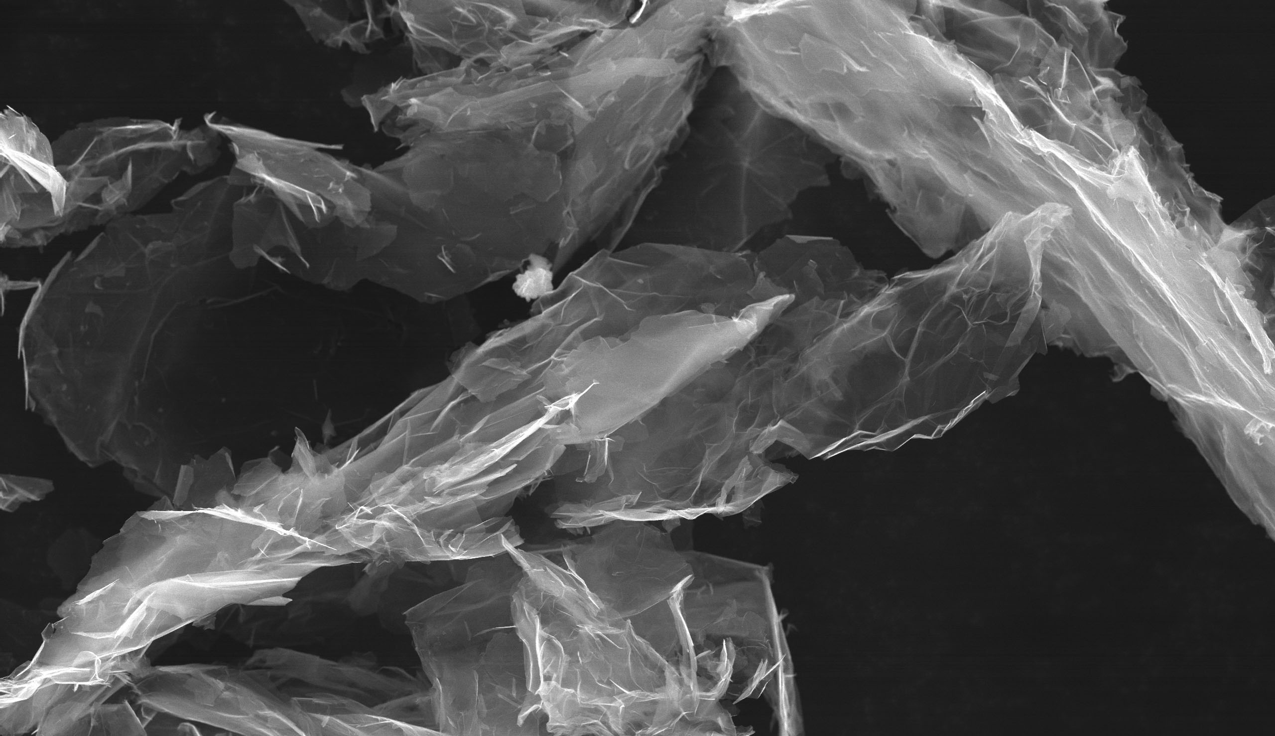
A traditional transistor exists in two states; on or off which in digital terms equals one or zero. This is a very basic form of logic called Boolean and works well with the current materials in use today. The problem comes as we shrink the size of transistors. As things get smaller the barriers between the pathways become thinner. If they are too thin the insulation intended to contain current leaks into the surrounding material. This leakage can cause excess heat and also logic errors if the leakage is too great. For example is a transistor is supposed to be closed, but appears to be open due to leakage you are going to get processing errors. With graphene this phenomenon is even worse as there is no barrier at all. This means that “closed” graphene circuits can appear as open which is not a good thing if you are trying to build a traditional transistor.
There have been solutions for this posited, including building an artificial barrier (also called a gap) to lock in the current. None of these have really worked as they cause a fundamental change in the way that graphene operates; simply put if you do something to overcome this, graphene loses the characteristics you want from it. This was the problem that the team from UCR were trying to tackle, but instead of finding a way to work against graphene’s amazing properties they used a judo move to work with it.
The team was electrical engineering professors Alexander Balandin and Roger Lake, adjunct professor of electrical engineering Alexander Khitun, and Guanxiong Liu and Sonia Ahsan (who earned their doctorate during this research). Together they decided that if they could not get graphene to work like traditional materials, it was time to change the transistor to match the properties of graphene. This meant ditching the “on/off” Boolean logic of traditional transistors and finding a way to make things work without it.
The leap of logic was not too great though as they found an analog in traditional computing. The new “non-Boolean” transistor works in a way that is very much like a diode connected MOSFET (metal-oxide-semiconductor field-effect-transistors). In a diode connected MOSFET you have two voltage inputs that then result in one voltage output. The team designed G-FETs (graphene-field effect transistors) in graphene using this type of logic. They attached a top gate and two back gates to the new G-FETs (again very much like a diode connected MOSFET). By having multiple inputs on a single output they were able to find their happy place and effect a new logic that will still work for current computing needs. In other words; although the logic is no longer single gate-on/off it still achieves the same results as existing transistor designs. Now this is a massive oversimplification on our part, but is still representative of the concept. If you want a much more detailed explanation of the UCR Team’s findings you can get them in PDF format.
With this new design they did not need to worry about setting up an energy gap and maintain all the qualities of graphene that make it a desirable material for building circuits. Of course more work needs to be done to validate this new concept at the nano-scale (these were “large” test circuits), but the work is very promising and could start a materials shift in the next few years as opposed to hitting the limit with CMOS (complementary metal-oxide semiconductor) technology in 10-12 years. At that time it is anticipated that the drive for sub-10nm transistors will exceed what CMOS can do. Intel should be very interested in this news as they are already heading for 14nm in their next designs and while their tri-gate transistors should carry them to 10nm it is unlikely that it will carry much farther than that.
Tell us what you think in our Forum

